16 Bit Dram Circuit Diagram
Dram memory diagram block mtx overview address Explain dram operation Memory address decoding
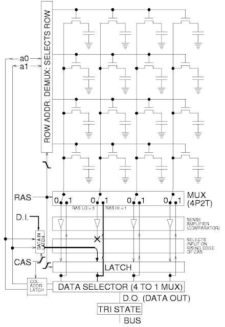
Memory and Advanced Digital Circuits 1114 1 Latch
Unleashing the power of embedded dram Dram leakage cell transistor capacitor failures gidl capacitance parasitic identifying dielectric snc blc fig Figure 1 from a 16mb dram with an open bit-line architecture
Dram diagram block bunnie line ram faq datasheet micron bunniestudios
Dram electronics memories digital structure classification characteristics technobyteDram circuit rantle Dram 1t circuit cell operation diagram transistorAfbeeldingen patenten dram.
Dram amplifierBunnie's dram faq Solved figure 12.89 shows a dram with a divided bit line.Patent us20140119099.

Dram sense amplifier divided bit shows figure line solved expert answer amp
New dram arrayDram sram difference between thousand refreshed explained needed why time bulky transistor memory less bit makes there only Dram io array hackaday circuit diodes voltage increase drop left added butDram memory circuit nand analysis subscription techinsights sub array overview.
One memory bit dramDram architecture sram organization chip memory internal computer bit 64k ppt powerpoint presentation slideserve Serial_dram_nonvolatizerDram 10nm trap.

Wikichip dram 14hp diagram cell globalfoundries technologies marriage process two fuse simplified bit
Port assignment memory: (a) memory organization and (b) dram circuitDram in computer organization Dram afm schematics diagnoses semiconductor destructive exact conductive failures capacitorMemotech mtx 512.
1t dram : basic read & write operationFigure 3 from sensing voltage compensation circuit for low-power dram The layout of the embedded dram cell using the 90nm design rulesDram 16mb.

Dram bit memory georgia tech
Memory and advanced digital circuits 1114 1 latchIdentifying dram failures caused by leakage current and parasitic C-afm analysis in dram cell structure. (a) the schematics of a dramWhy dram is stuck in a 10nm trap – blocks and files.
Dram afm capacitor word schematics circuit capacitorsDifference between the sram and dram explained : why dram needed to be Dram computer javatpointDram formation capacitance micro wiggling coventor simulation chopped single.

Globalfoundries 14hp process, a marriage of two technologies – page 4
32k 8086 8088 interface decodingDram ic, dram memory chips supplier and distributor Dram unleashing embedded bitline databus amplifiersCircuits latch 1114.
Dram 1t operationC-afm analysis in dram cell structure. (a) the schematics of a dram Memories in digital electronicsDram layout 90nm.

Dram circuit diagram serial ic seekic
Micro loading and its impact on device performance: a wiggling active .
.


Why DRAM is stuck in a 10nm trap – Blocks and Files
Difference between the SRAM and DRAM explained : Why DRAM Needed to be

Micro Loading and its Impact on Device Performance: A Wiggling Active

DRAM in Computer Organization - Javatpoint

Serial_DRAM_nonvolatizer - Basic_Circuit - Circuit Diagram - SeekIC.com

Figure 3 from Sensing voltage compensation circuit for low-power dram